


Stringent Requirements for Semiconductor Tooling Fixtures
In the semiconductor manufacturing field, the performance of tooling fixtures directly impacts product quality and production efficiency. These tools must simultaneously meet multiple stringent standards: high cleanliness ensures no contamination, high dimensional stability guarantees precision, high-temperature resistance adapts to process environments, and chemical corrosion resistance handles cleaning processes. Additionally, rapid iteration capabilities, cost control, and compatibility with automated production lines are equally essential.
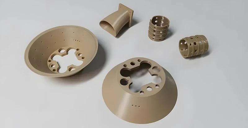
Tower Semiconductor, as a global leader in specialty process wafer foundry services, has extensive demands for specialized tooling in core businesses such as MEMS, 300mm wafer manufacturing, silicon photonics, and high-end analog chips: wafer handling fixtures, robotic arm end effectors, vacuum environment insulation components, high-temperature process fixtures, and ESD anti-static functional components.
Limitations of Traditional CNC Machining in Low-Volume Scenarios
For low-volume, customized semiconductor tooling requirements, traditional CNC machining faces numerous challenges:
| Pain Points | Typical Situation |
|---|---|
| Long delivery cycles | 7–21 days |
| High per-unit costs | $300–$3000 |
| Complex structure limitations | Internal channels difficult to machine |
| High design iteration costs | Each modification requires re-machining |
CreatBot PEEK-300 high-temperature PEEK additive manufacturing technology provides effective solutions to the above problems.
CreatBot PEEK-300 Technical Specifications
| Parameter | CreatBot PEEK-300 |
|---|---|
| Nozzle temperature | Up to 500°C |
| Bed temperature | Up to 200°C |
| Constant temperature chamber | Up to 120°C |
| Build volume | 300 × 300 × 400 mm |
| Supported materials | PEEK / PEKK / PEI / PPSU / Carbon fiber composites |
| Print precision | ±0.1 mm |
| Continuous operation capability | Supports 72+ hours industrial continuous printing |
Typical Application Scenarios
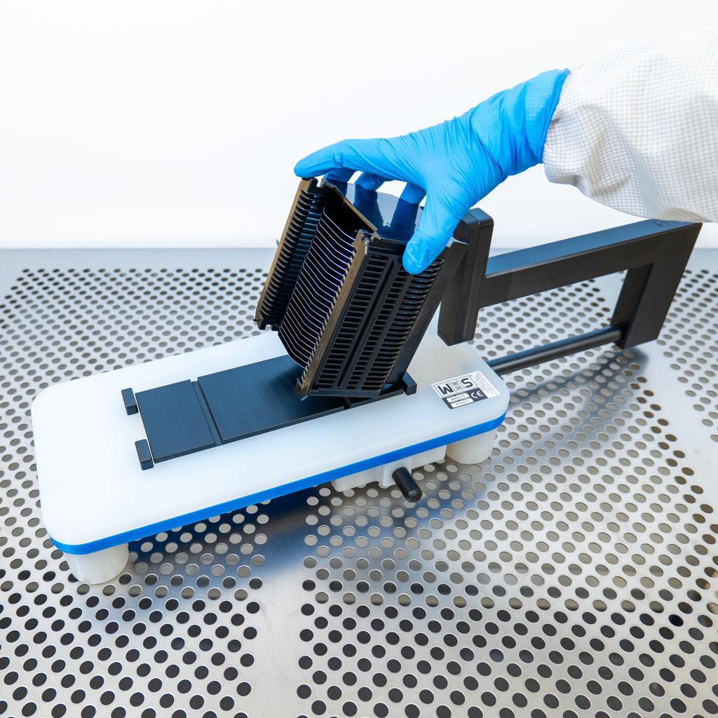
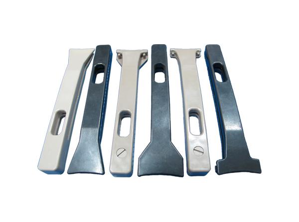
1. Wafer Handling Fixtures
Wafer handling systems have extremely strict precision requirements for tooling. Dimensional tolerances typically need to be controlled within ±0.05–0.1 mm, while also enduring long-term 120–200°C operating temperatures, IPA and various acid-base cleaner corrosion, and mechanical stress from high-frequency automated cycles.
Core Performance of PEEK Material
| Performance Indicator | Test Data |
|---|---|
| Long-term use temperature | 250°C |
| Tensile strength | 90–100 MPa |
| Chemical corrosion resistance | Excellent |
| Water absorption | <0.1% |
| Flame retardant rating | UL94 V-0 |
Application Case: Wafer Positioning Fixture
| Comparison Dimension | CNC Machining | PEEK-300 Printing |
|---|---|---|
| Production cycle | 10 days | 8 hours |
| Per-unit cost | $850 | $90 |
| Finished weight | 420 g | 210 g |
| Structural complexity | Medium | High |
2. Semiconductor Automated Robotic Arm Fixtures
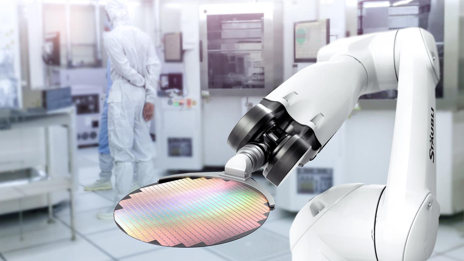
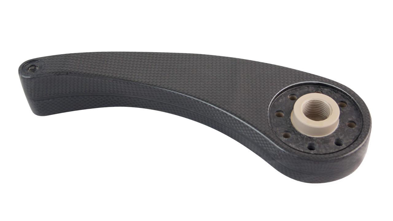
In wafer fab automated production lines, key components such as Robot End Effectors, Vacuum Grippers, Sensor Holders, and ESD Fixtures require frequent design adjustments based on process changes.
Bottlenecks of traditional machining methods: Single tooling modification cycles typically take 5–14 days, severely impacting automated debugging efficiency.
Advantages of PEEK-300 solution:
| Key Indicator | Improvement |
|---|---|
| Tooling development cycle | Reduced by 70–90% |
| Single verification speed | Improved by approximately 5x |
| Low-volume manufacturing cost | Reduced by 60–80% |
| Fixture weight | Reduced by 30–50% |
3. Vacuum Environment Insulation Components
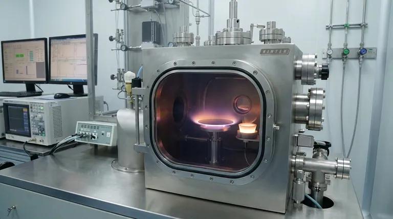
In semiconductor process equipment such as CVD, PVD, Plasma Etching, and MEMS, ordinary engineering plastics often face issues like outgassing, thermal deformation, and chemical corrosion.
Performance of PEEK in vacuum environments:
| Application Environment | Performance Characteristics |
|---|---|
| Vacuum environment | Low outgassing rate |
| High-temperature environment | 250°C long-term stable operation |
| Chemical environment | Acid and alkali corrosion resistant |
| High-frequency operation | Excellent dimensional stability |
PEEK Additive Manufacturing vs Traditional CNC Machining
| Comparison Dimension | CNC Machining | PEEK 3D Printing |
|---|---|---|
| Low-volume cost | High | Low |
| Complex structures | Design limited | High design freedom |
| Internal channels | Difficult to machine | Easy to implement |
| Iteration speed | Slow | Fast |
| Automation compatibility | Average | Excellent |
Core Value of CreatBot PEEK-300
- Tooling development cycle reduced by up to 90%
- Low-volume manufacturing costs reduced by 60–80%
- Automated fixture weight reduced by up to 50%
- Complex functional structures quickly realized
- Meets cleanroom high-performance material standards
With the rapid development of AI chips, MEMS, silicon photonics, advanced packaging and other technologies, the semiconductor industry's demand for high-performance engineering plastics and industrial-grade additive manufacturing solutions continues to grow.
With its 500°C high-temperature nozzle, 120°C constant temperature chamber, PEEK/PEI and other engineering material support, and industrial-grade long-term stable printing capabilities, CreatBot PEEK-300 is providing advanced semiconductor manufacturing enterprises with more efficient and flexible tooling manufacturing solutions.


